Research
Raman spectroscopy and microscopy
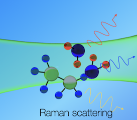
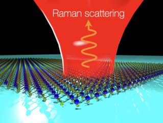
When a photon of specific energy falls on a molecule, it can deliver a small part of its energy to the molecule and scatter away with the remaining energy. This process is known as Raman scattering. After receiving energy, the molecule would start to vibrate and go into a higher vibrational energy state. The molecule can receive only a certain amount of energy that matches its vibrational energy levels, which would depend on the characteristic of that particular molecule. The energy received by the molecule would be the same as the energy lost by the photon, which can be calculated by measuring the energy of the scattered photon and by subtracting it from the energy of the incoming photon. This measurement process is called Raman spectroscopy. Therefore, Raman spectroscopy can tell us all about the possible vibrational energies of a molecule, or in other words, it can identify a molecule through its intrinsic properties. Similarly, if one shines light to a sample containing a large number of molecules, one can obtain vibrations energies of all possible inter- and intra-molecular vibrations of the sample and hence identify all constituent molecules and their chemical bonds. Raman spectroscopy, therefore, provides us a wonderful nondestructive and noninvasive tool to study various chemical, physical and biological properties of a sample that have their signatures in vibrational spectra. Usually, a laser beam of specific energy is tightly focused on the sample to invoke Raman scattering from a tiny volume of the sample. If a sample is large, the laser focus spot can be scanned over the sample to measure Raman scattering from the entire sample, and then any of the intrinsic properties of the sample can be spatially mapped across the sample. This process, which effectively makes an image of the spatial distribution of some intrinsic property of the sample, is known as Raman imaging or Raman microscopy. If various intrinsic properties of a sample are color-coded in a Raman image, one can obtain a color optical image of the sample with rich information about the spatial distribution of those properties where each color would represent the distribution of one particular property. We utilize Raman spectroscopy and microscopy not only to analyze various samples to visualize and reveal their novel characteristics, but also as the basic tool used in many other interesting techniques that we develop.
Applications of Raman spectroscopy and microscopy
Other than the usual characterization, Raman scattering can reveal many interesting properties of various samples, which other methods cannot observe. We, therefore, utilize Raman spectroscopy and microscopy to study many kinds of samples, such as carbon nanotubes, graphene, organic semiconductors, two-dimensional transition metal dichalcogenide materials, biological materials, and many more. Furthermore, we have been developing Raman technique in our own innovative ways, for example, to measure extremely low-frequency Raman scattering that reveals weak intermolecular van-der-Waals interactions, or to introduce a home-built cryo-chamber to understand temperature-dependent variations in molecular interactions. We utilize various incident light from the high-energy photons to the low-energy photons in our Raman studies. Furthermore, we are also working with infrared absorption spectroscopy by building an FTIR system to compare it with Raman scattering.
Tip-enhanced Raman scattering (TERS) microscopy
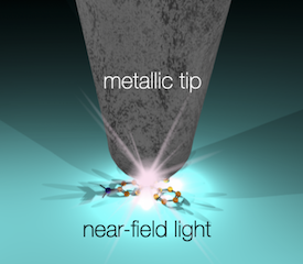
The wave nature of light prevents it from focusing down to an area smaller than about half of its wavelength, a phenomenon known as the diffraction limit of light. Therefore, optical microscopy with visible light cannot achieve a spatial resolution better than about 200~300 nm. However, near-field techniques that involve imaging samples in close proximity of a metallic nanostructure have ways to overcome this diffraction limit. One of such techniques, known as tip-enhanced Raman scattering (TERS), utilizes a metallic nano-tip with a sharp apex of the order of tens of nanometers as the imaging probe. When such a metallic nano-tip is illuminated with propagating light, it creates a so-called nano-light-source containing evanescent (non-propagating) light that is strongly enhanced and tightly confined within a volume comparable to the size of the tip apex, also known as the near-field light. Thus, the tip can illuminate the sample with a nano-sized confined light, even with a visible frequency, and invoke Raman scattering from a nanometric volume of the sample. TERS microscopy, therefore, goes beyond the classical limits not only in achieving super high spatial resolution by jumping far beyond the diffraction limit of light, but also in achieving new exciting results by combining it with other analytical techniques, such as nonlinear spectroscopy or the application of unidirectional local pressure to the samples. We have not only utilized TERS microscopy to analyze various interesting samples at the nanoscale, but have also been actively involved in developing new technological improvements in TERS microscopy itself to achieve new goals and further improve detection sensitivity, measurement stability and reproducibility, spatial resolution and imaging speed to bring it up to the next level. Also, imaging based on photoluminescence can be benefited by the near-field effects at the sharp apex and one can complement TERS with microscopy based on tip-enhanced photoluminescence.
Plasmon nanofocusing for near-field optical microscopy
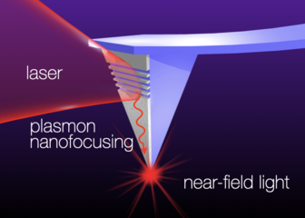
A traditional scattering-type near-field microscopy, including TERS microscopy, utilizes near-field light generated through the process of plasmon resonance at the apex of a nano-tip. This process, which requires direct illumination of the tip apex, inevitably also involves illumination of the sample right beneath the tip apex within a focal volume. Therefore, the near-field optical signal generated from the sample's nanometric volume is also accompanied by a far-field optical signal generated from a much larger volume of the sample within the laser focus spot, which constitutes an unwanted background signal. This background scattering signal in TERS can, however, be later subtracted by measuring it independently after taking the tip away. While this double measurement process works well for most practical purposes, it essentially ignores weak Raman signals that might remain buried within the far-field background. Plasmon nanofocusing is another technique to create an enhanced and highly confined near-field light at the tip apex, where the incident light is spatially well-separated from the tip apex. This eliminates the need to shine incident light directly on the sample and thus, there is no far-field background signal generated in this technique. This process is a non-resonant phenomenon, where a plasmon coupler, usually in the form of a grating, is fabricated at the tip body far from the apex. When this coupler is illuminated with laser light, the light energy is coupled with the plasmons, and then the excited plasmons propagate towards the tip apex by focusing and adiabatically compressing their energy to the tip apex, where they create an enhanced and tightly confined near-field light. When near-field microscopy is performed with this nano-light-source created by plasmon nanofocusing, one can observe pure near-field signals without any involvement of the far-field background. The phenomenon of plasmon nanofocusing has been known for a while, however, we have developed our own well-improved technique with specially designed innovative nano-tip for efficient plasmon nanofocusing. We are continuously improving this technique further and utilizing it for TERS, near-field photoluminescence and other near-field optical microscopic studies.
Broadband plasmon nanofocusing for white nano-light source
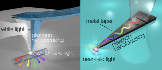
Plasmon nanofocusing is an interesting way to create a background-free nano-light-source, where plasmons propagate on a tapered metallic nanostructure or on the surface of a metallic nano-tip and eventually nanofocus to create an enhanced and tightly confined near-field light at the apex of the structure. Unlike the traditional scattering-type near-field microscopy, plasmon nanofocusing is not based on plasmon resonance, and is therefore independent of the incident wavelength. This means, while plasmon resonance-based generation of near-field light works only for a narrow wavelength range near the resonance, plasmon nanofocusing-based generation of near-field light would work for a broadband wavelength range, resulting in the generation of a white nano-light-source. Although the phenomenon of plasmon nanofocusing itself is independent of incident wavelength, the plasmon coupler can only couple a particular wavelength efficiently, making the whole process effectively a wavelength-dependent process. To overcome this hurdle, we have come up with a simple but innovative design of the plasmon coupler that can couple all wavelengths, and we can therefore obtain white nano-light-source through broadband plasmon nanofocusing. We have developed this technique of broadband plasmon nanofocusing not only for TERS nano-tips, but also for tapered metallic nanostructures fabricated on a substrate for its multidimensional applications, including for wavelengths ranging from ultraviolet to far-infrared. We have been developing novel optical technologies with broadband plasmon nanofocusing such as multi-wavelength super-resolution imaging technique, optical sensor, optical nano-trapping and so on.